This is a step by step guide to installing the SNES RGB Bypass + Dejitter mod on a SNS-CPU-1CHIP-01. This guide is also applicable to the SNS-CPU-1CHIP-02 and SNS-CPU-1CHIP-03 with only minor differences.
Basic Installation:
The basic installation procedure for the SNES 1CHIP. offers the core features that most users will want from their SNES RGB Bypass + Dejitter mod on the SNES 1CHIP. These main features include:
– RGB Bypass. This part of the mod bypasses the RGB output of the SNES 1CHIP providing superior image quality.
– Csync Restore. This part of the mod restores Csync to the SNS-CPU-1CHIP-03.
– Csync Dejitter. This part of the mod adds the dejitter functionality to the SNES 1CHIP Csync output.
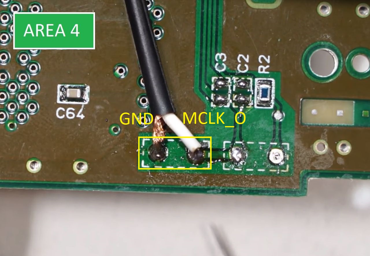
Installation Overview Image.
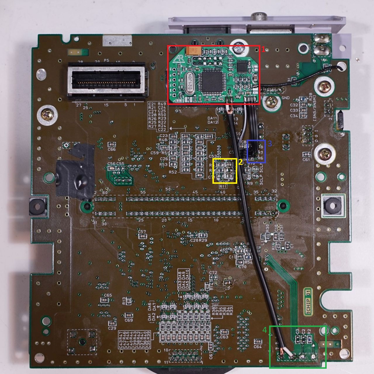
The areas of interest are numbered and color coded.
Red is area 1
Yellow is area 2
Blue is area 3
Green is area 4
Basic Installation Procedure:
Step 1: Remove the 6 gamebit screws from the SNES 1CHIP shell. You need to use a 4.5mm gamebit screwdriver for this.
Step 2: Remove all Phillips head screws from the motherboard and and power switch. Remove eject lever and the motherboard from the shell.
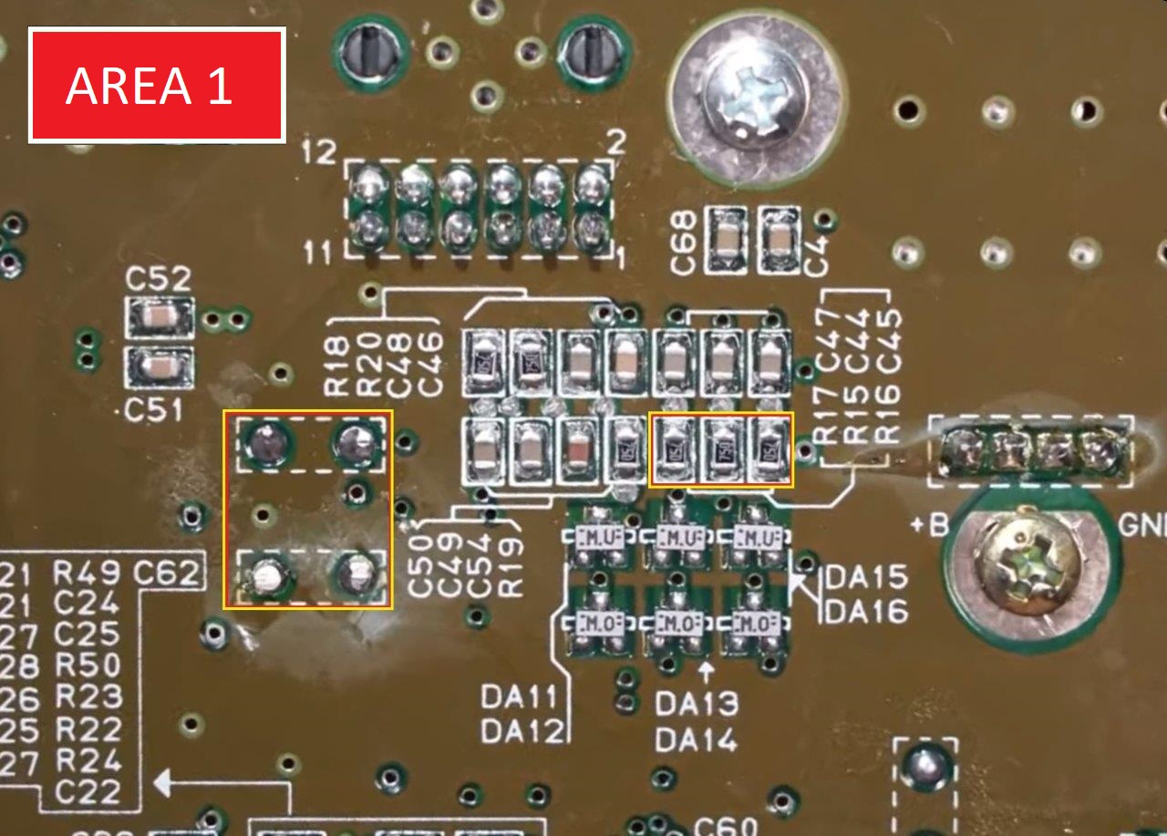
Step 3: Locate and trim the legs of the capacitors the back side of the SNES 1CHIP. motherboard near the AV Multi Out port. Remove R15,16, and 17. These areas are outlined in the image below.
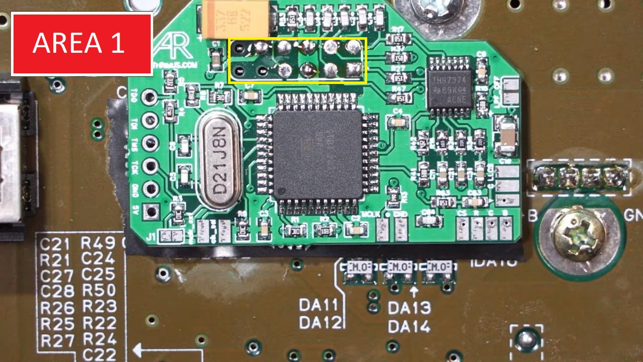
Step 4: Place the SNES RGB Bypass + Dejitter mod onto the pins of the AV Multi Out as shown in the photo below.
Step 5: Remove the crystal (X1) from the motherboard. There are a few ways to do this depending on what soldering equipment you have available. The way I do it is to use a large soldering iron tip and add plenty of extra solder to both legs of the X1 crystal keeping the solder molten across both legs. Usually the X1 crystal will fall off of the motherboard under it’s own weight if you can keep both legs hot enough. If you do not have a large enough soldering tip, you could remove the solder from the legs of X1 using a solder sucker, desoldering gun, or desoldering braid. Do whatever you are comfortable with.
You must also remove C3 from the motherboard. Check the outlined components in the image below.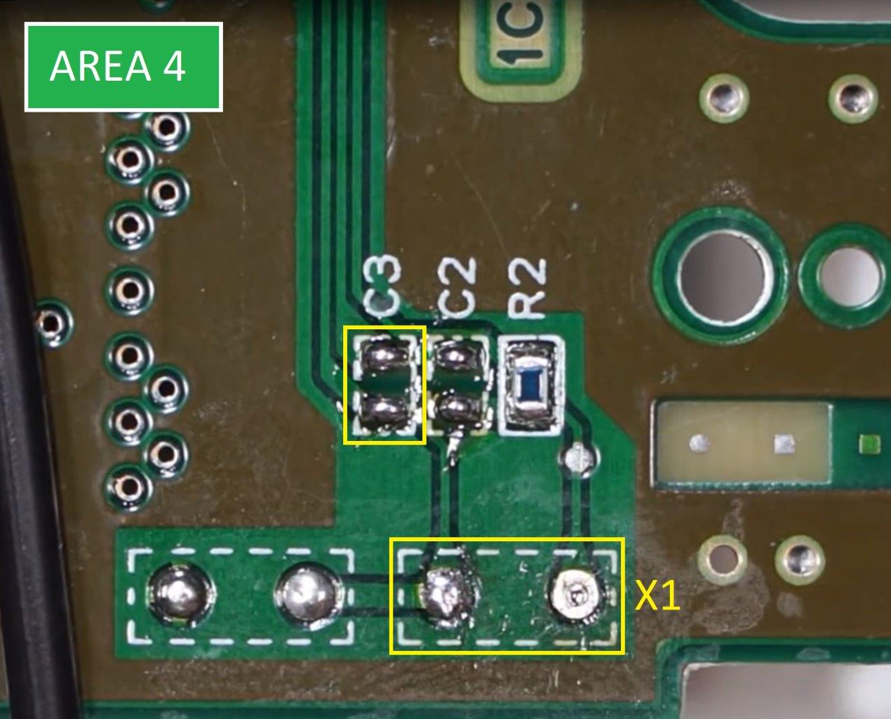
Step 6: Remove R12 from the SNES 1CHIP motherboard.
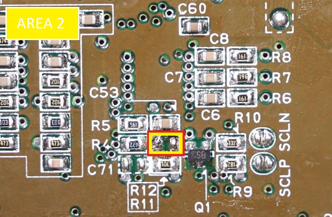
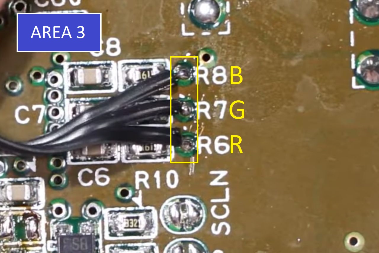
Step 7: Solder your R,G, and B wires to the vias next to R6,7, and 8.
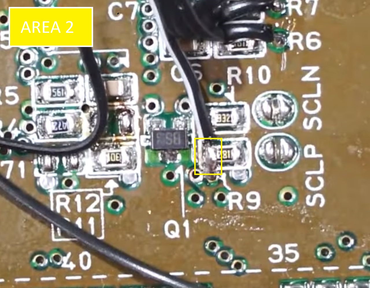
Step 8: Solder your Csync wire to the left side pad of R9.
Step 9: Solder you Csync, R, G, and B wires to the corresponding pads on the RGB Bypass + Dejitter Board.
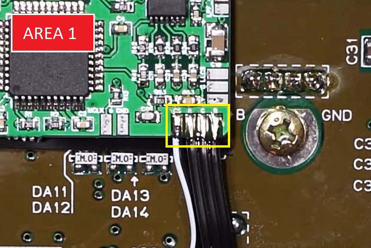
Step 10: Solder a wire to MCLK_O. It is recommended that you use shielded cable for this, but it is not absolutely required. If you use shielded cable you need to solder the shielding to the GND pad right next to the MCLK_O pad. If you don’t use shielded cable you only need to solder a wire to the MCLK_O pad, and the GND pad is not used.
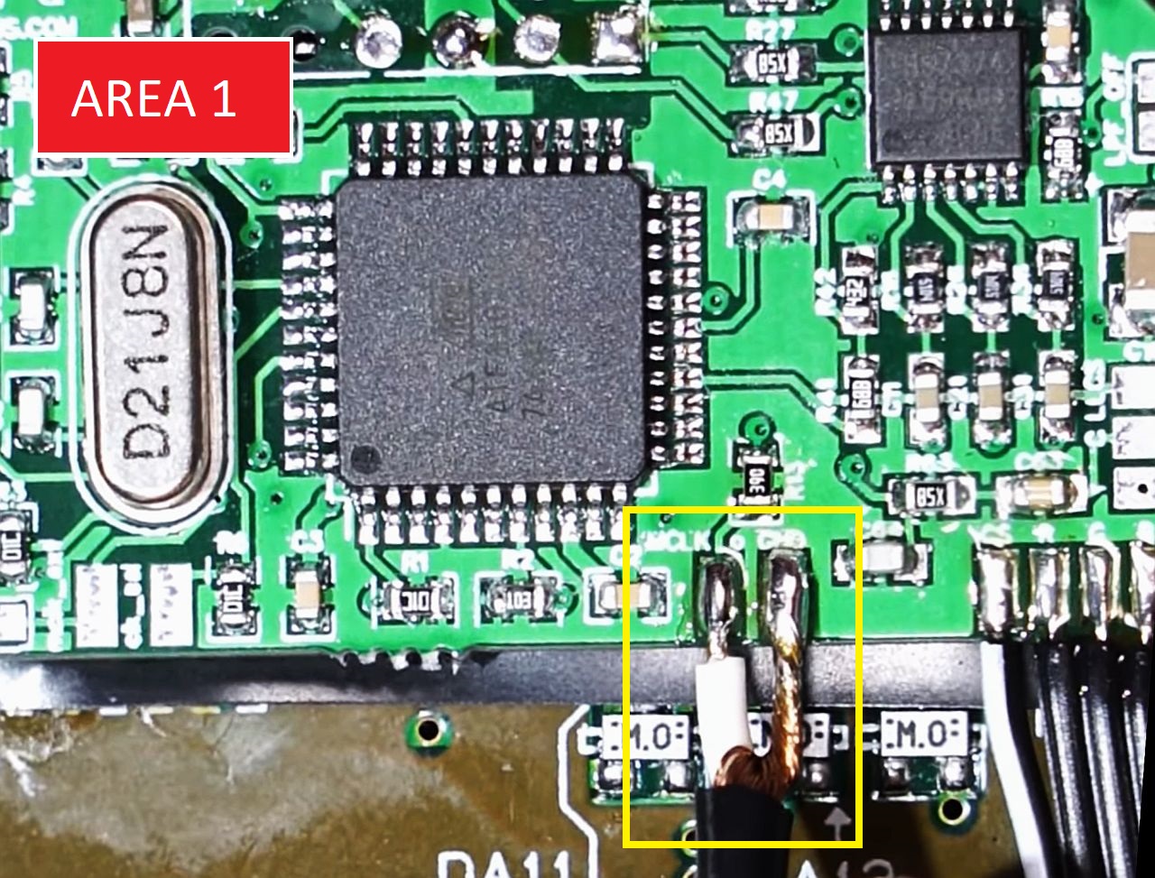
Step 11: Solder your MCLK_O wire to the via indicated in the image below. If you are using shielded cable you can solder GND to the via to the left of where you soldered the MCLK_O wire.
Step 12: Reassemble your SNES and enjoy!
Advanced Installation.
Coming soon!