Basic Installation:
The basic installation procedure for the SNES Jr. offers the core features that most users will want from their SNES RGB Bypass + Dejitter mod on the SNES Jr. These main features include:
– RGB Bypass. This part of the mod adds RGB output to the SNES Jr.
– Csync Restore. This part of the mod adds Csync output to the SNES Jr.
– S-Video Restore. This part of the mod adds S-Video output back to the SNES Jr.
– Csync Dejitter. This part of the mod adds the dejitter functionality to the SNES Jr. Csync output.
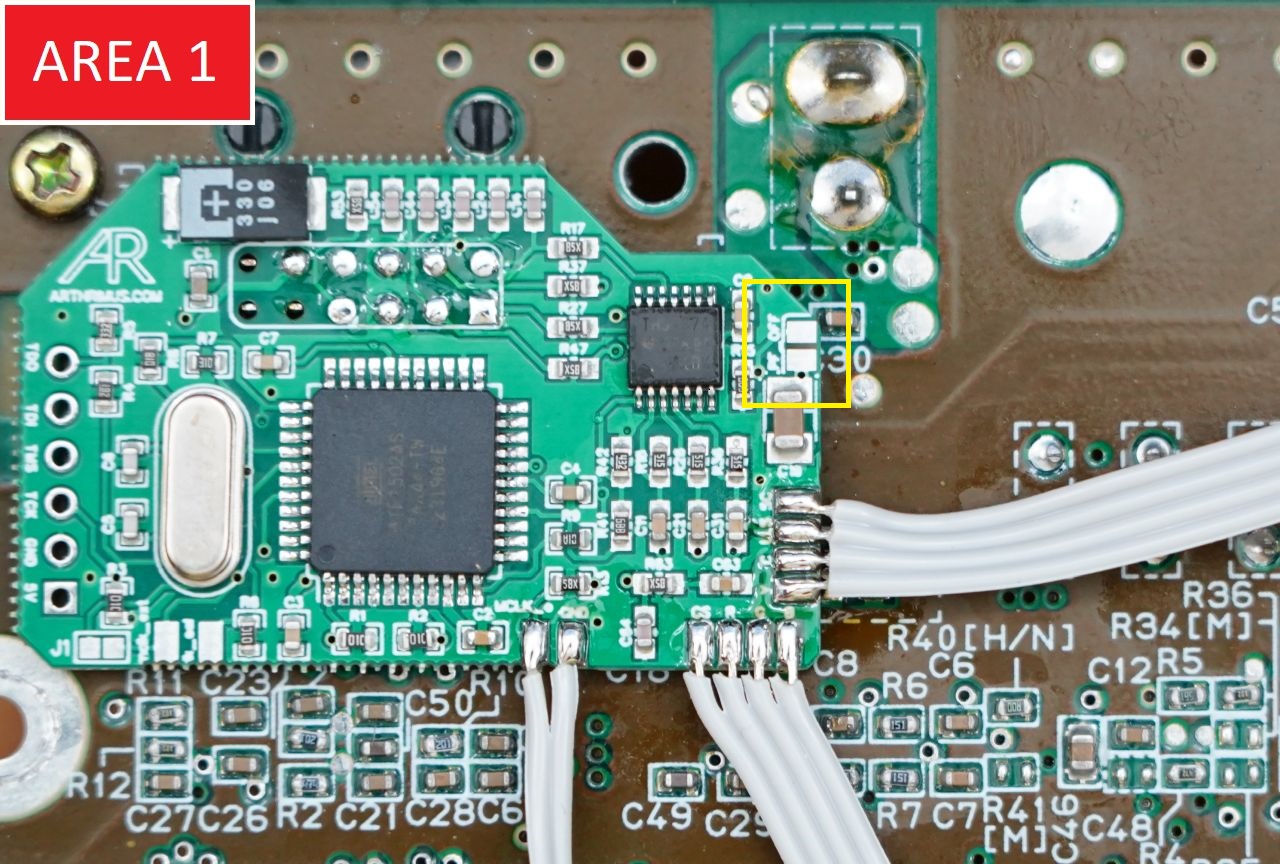
Installation Overview Image:
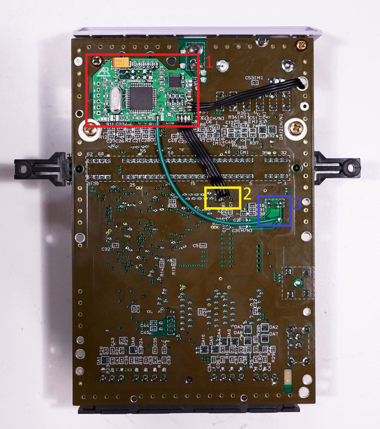
The areas of interest are numbered and color coded.
– Red is area 1
– Yellow is area 2
– Blue is area 3
Basic Installation Procedure:
Step 1: Remove the four gamebit screws from the SNES Jr. shell. You need to use a 4.5mm gamebit screwdriver for this.
Step 2: Remove all 7 Phillips head screws from the motherboard and remove the motherboard from the shell.
Step 3: Locate and trim the legs of the capacitors and the 7805 regulator on the back side of the SNES Jr. motherboard near the AV Multi Out port.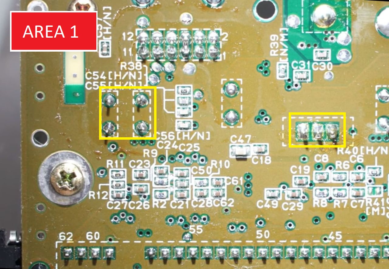
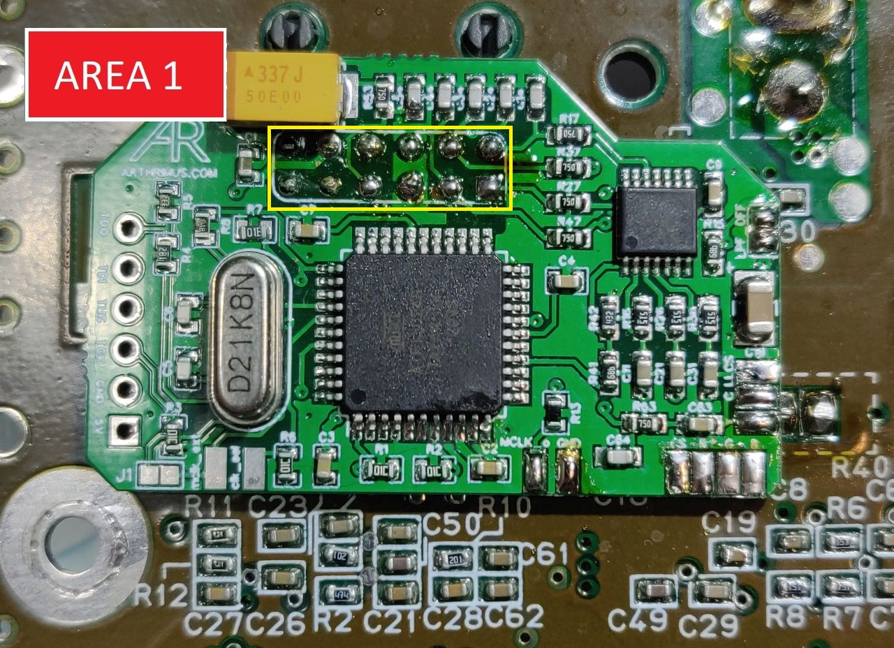
Step 4: Place the SNES RGB Bypass + Dejitter mod onto the pins of the AV Multi Out as shown in the photo below.
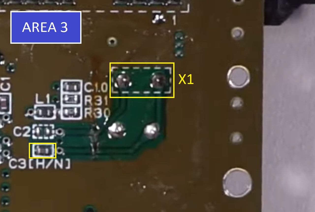
Step 5: Remove C3 and the crystal (X1) from the motherboard. There are a few ways to do this depending on what soldering equipment you have available. The way I do it is to use a large soldering iron tip and add plenty of extra solder to both legs of the X1 crystal keeping the solder molten across both legs. Usually the X1 crystal will fall off of the motherboard under it’s own weight if you can keep both legs hot enough. If you do not have a large enough soldering tip, you could remove the solder from the legs of X1 using a solder sucker, desoldering gun, or desoldering braid. Do whatever you are comfortable with.
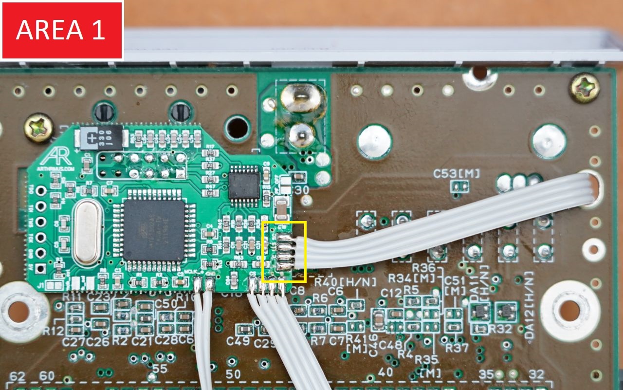
Step 6: Solder your Csync R,G, and B wires to the vias indecated below.
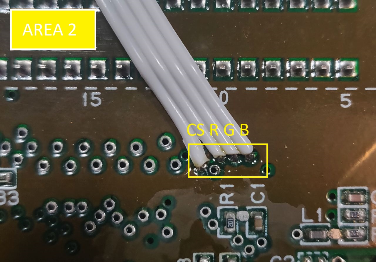
Step 7: Solder you Csync, R, G, and B wires to the corresponding pads on the RGB Bypass + Dejitter Board.
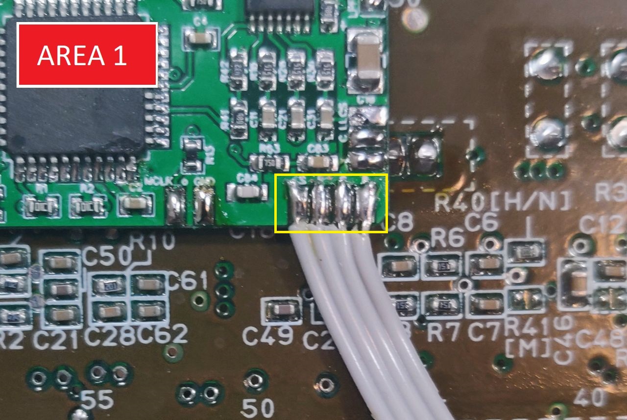
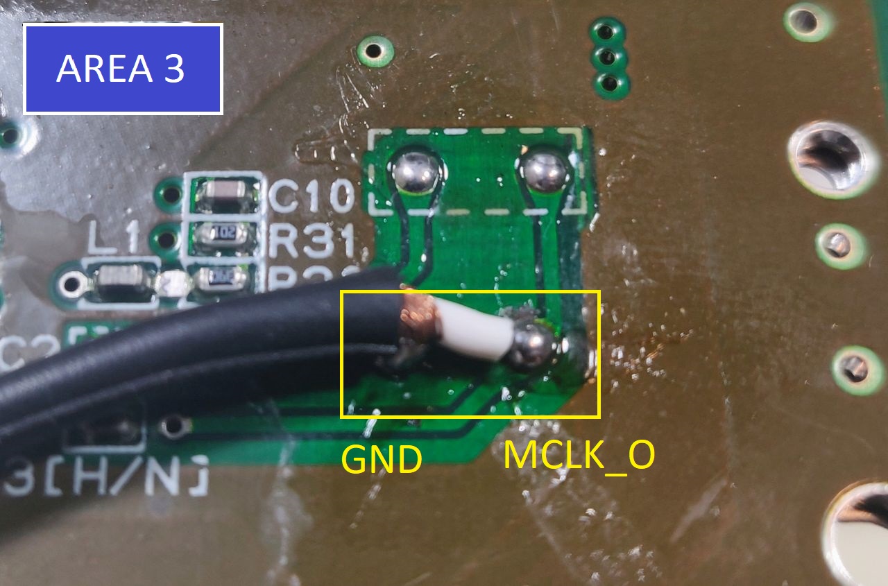
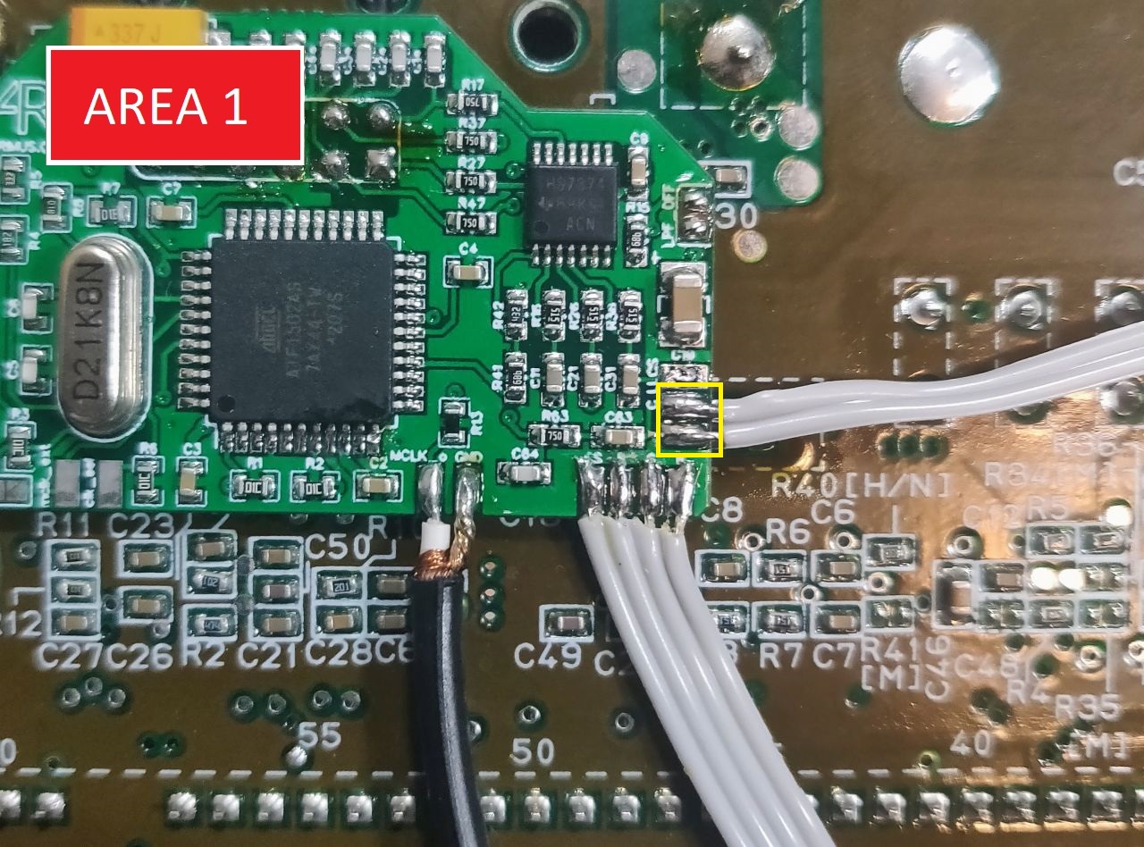
Step 8: Solder a wire to MCLK_O. It is recommended that you use shielded cable for this, but it is not absolutely required. If you use shielded cable you need to solder the shielding to the GND pad right next to the MCLK_O pad. If you don’t use shielded cable you only need to solder a wire to the MCLK_O pad, and the GND pad is not used.
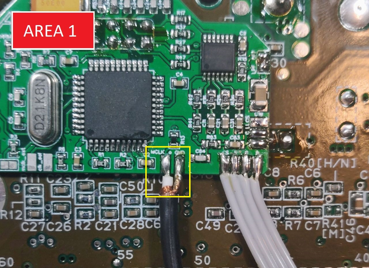
Step 9: Solder your MCLK_O wire to the via indicated in the image below. If you are using shielded cable you can solder GND to the via to the left of where you soldered the MCLK_O wire.
IF YOU ARE PLANNING TO DO THE ADVANCED INSTALLATION METHOD THEN STOP HERE AND PROCEED TO THE ADVANCED INSTALLATION SECTION.
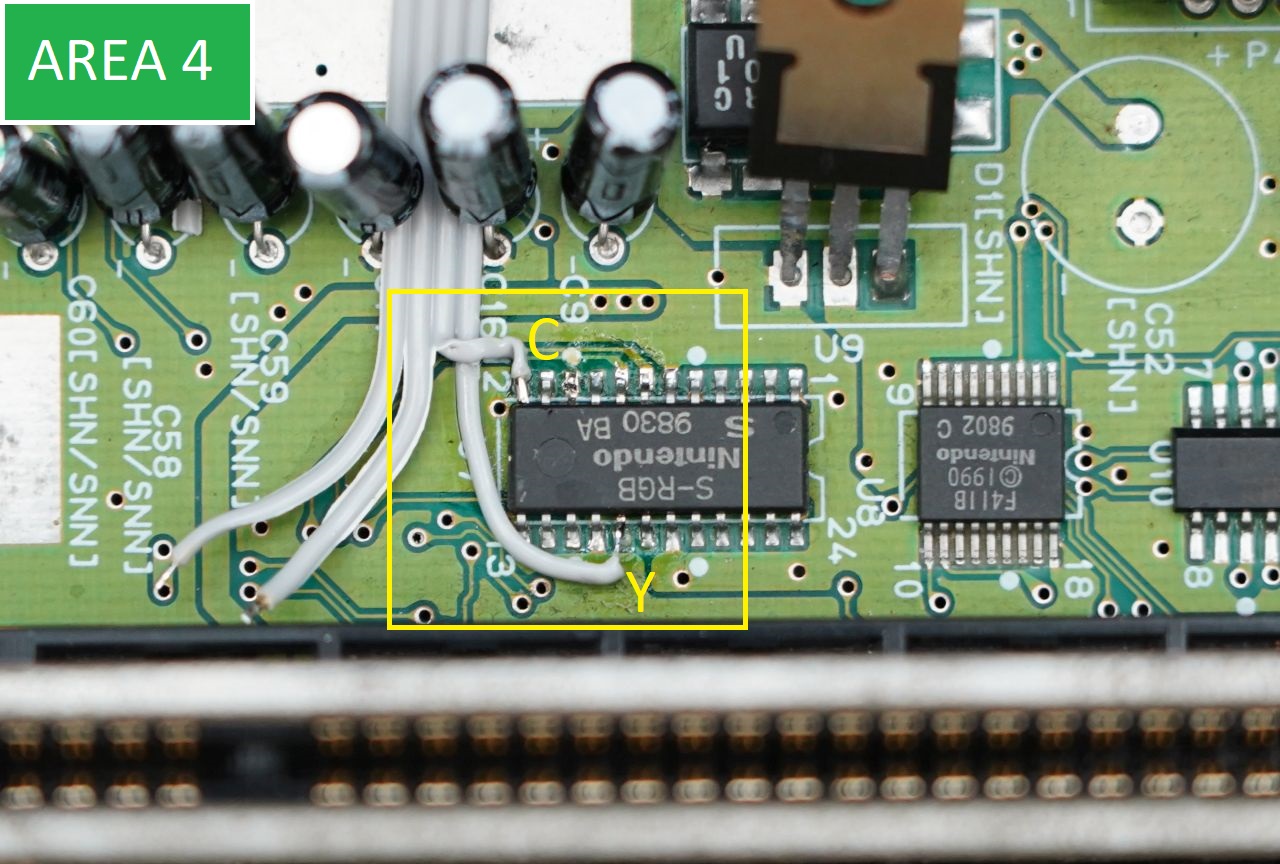
Step 10: Solder wires to the Y and C pads on the RGB Bypass + Dejitter Board.
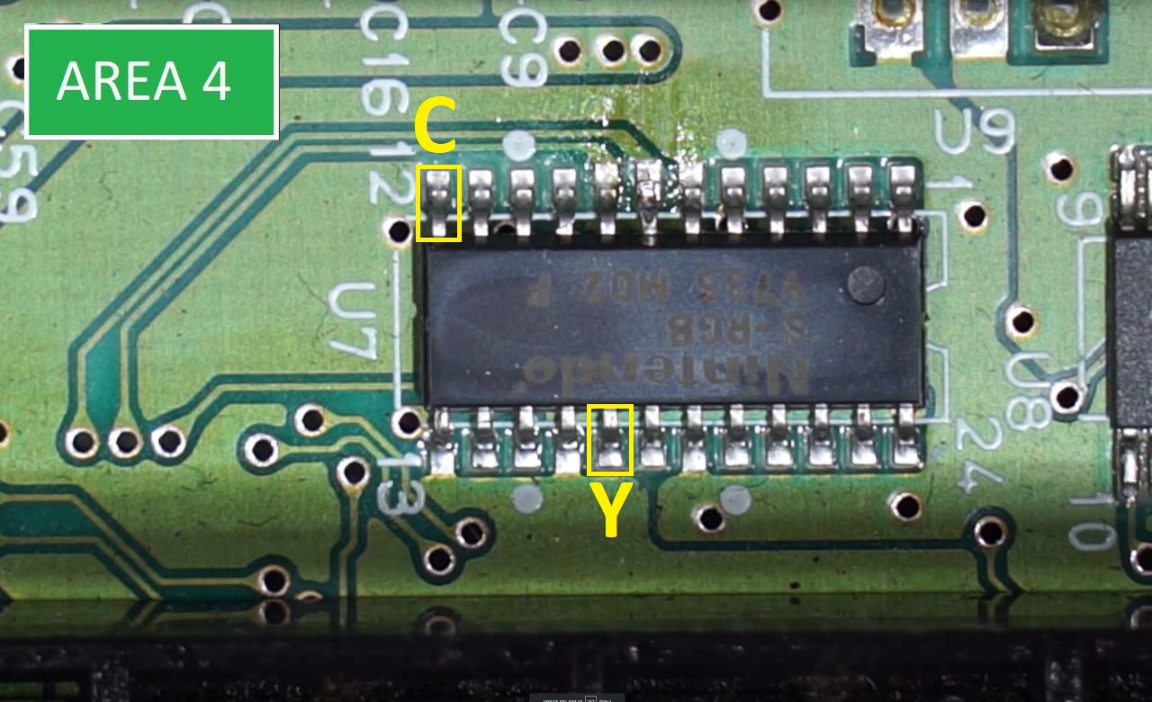
Step 11: Flip your SNES motherboard over and locate the S-RGB encoder chip above the cartridge slot. You should remove the heat sink from the 7805 voltage regulator so you have easier access to the S-RGB chip. Solder the Y wire to pin 17 and the C wire to the pin 12 of the S-RGB chip as indicated below.
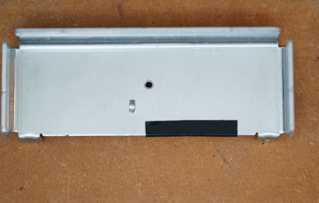
Once you are finished soldering the S-Video wires, you should add some electrical tape to the 7805 heatsink as shown below to prevent any possible shorts.
Step 12: Reassemble your SNES and enjoy!
Advanced Installation.
The advanced installation adds dejittered Composite Video and S-Video output. The advanced installation follows all of the same steps as the basic installation until step 10 where the installation deviates requiring additional wiring.
Note, this is an advanced install, requiring you to carefully lift multiple legs of the S-RGB encoder chip without breaking them. Do not proceed if you are not confident in your ability to successfully do this.
We will now pick up at step 10 and then continue from there.
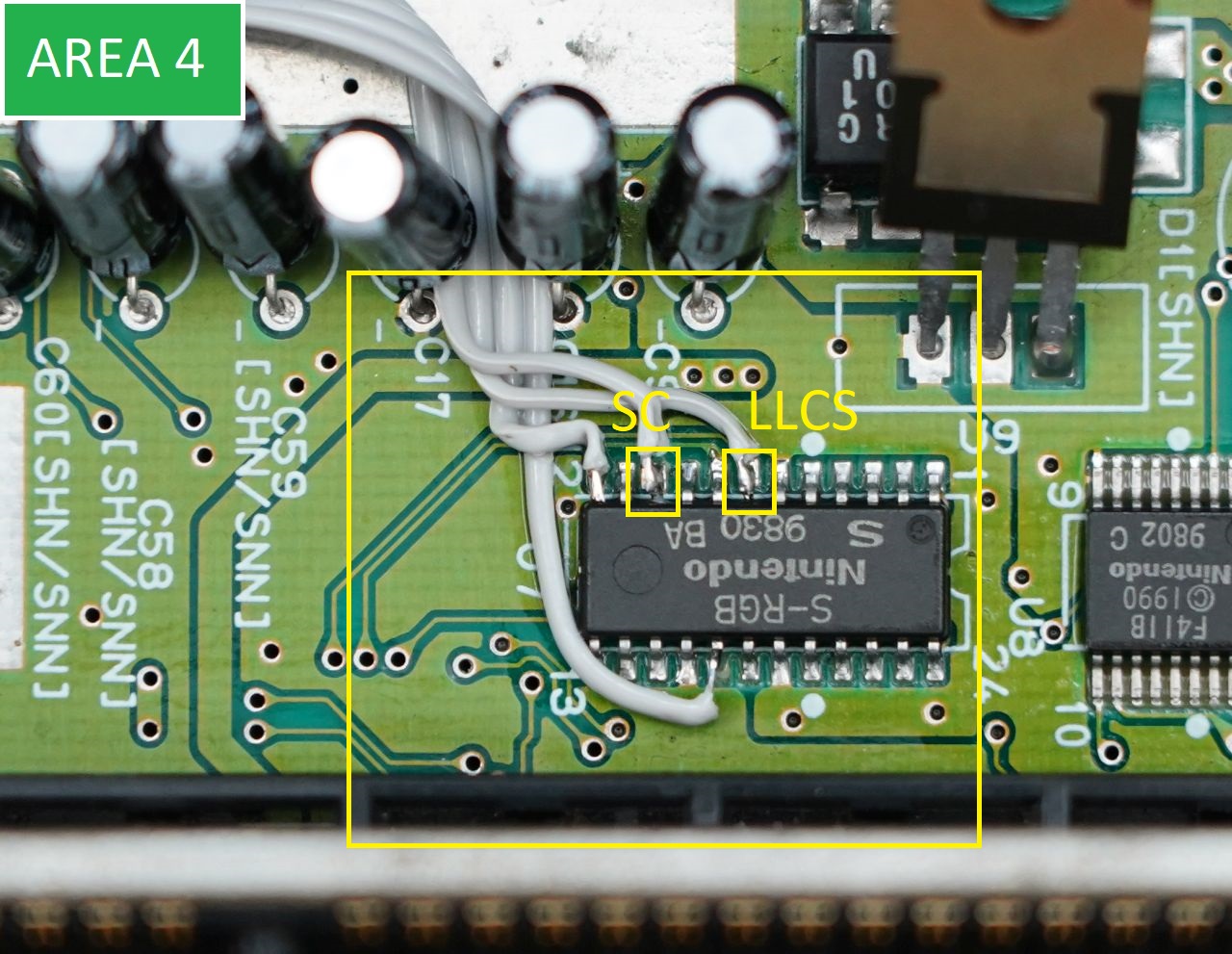
Step 10:Solder wires to the Y, C, LLCS, and SC pads on the RGB Bypass + Dejitter Board. Route your wires through the oblong hole on righthand side of the motherboard as shown below.
Step 11: Flip your SNES motherboard over and locate the S-RGB encoder chip above the cartridge slot. You should remove the heat sink from the 7805 voltage regulator so you have easier access to the S-RGB chip. Identify the following pins on the S-RGB encoder Pin 7 = LLCS, Pin 10 = SC, Pin 12 = C, Pin 17 = Y.
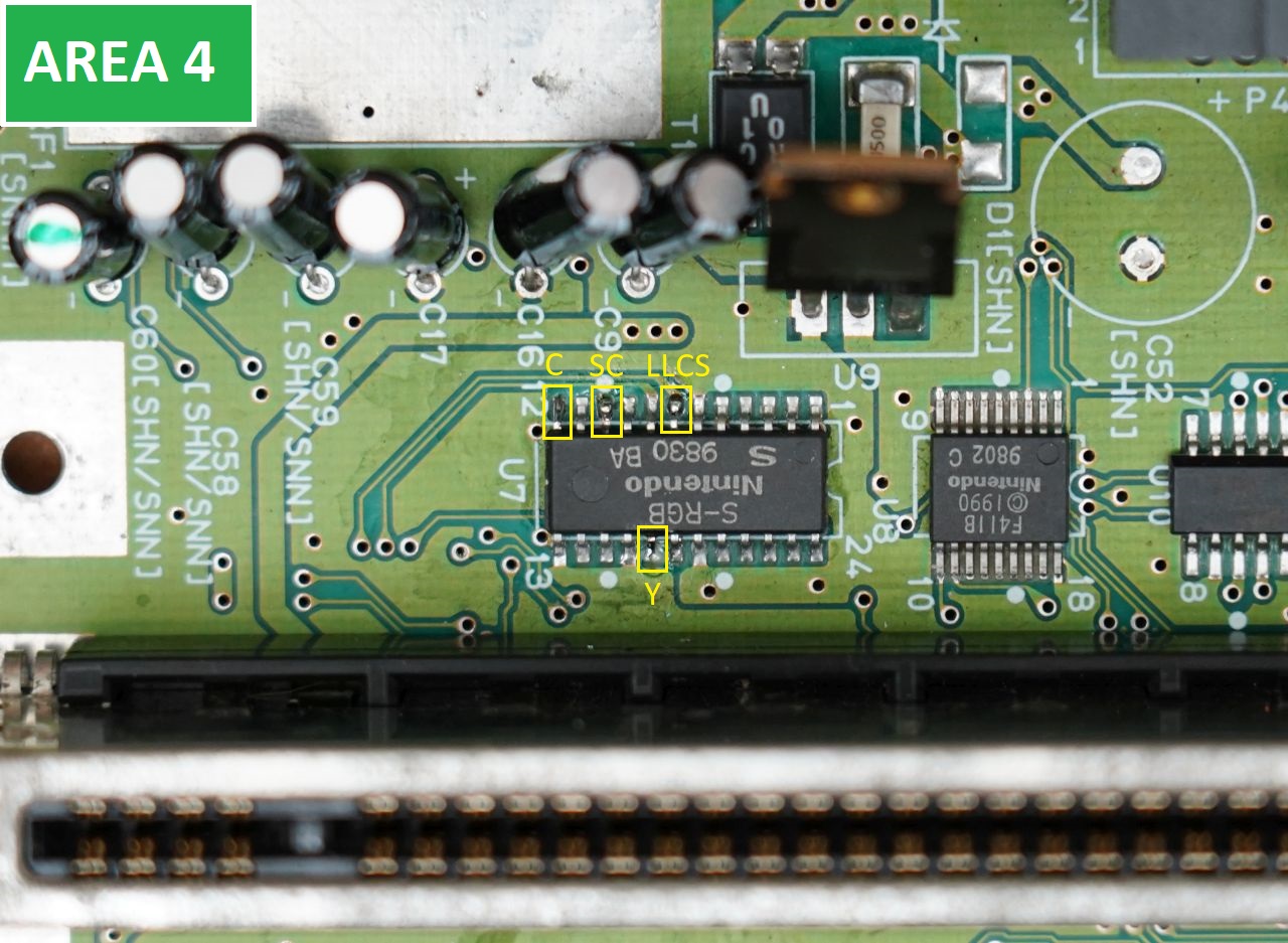
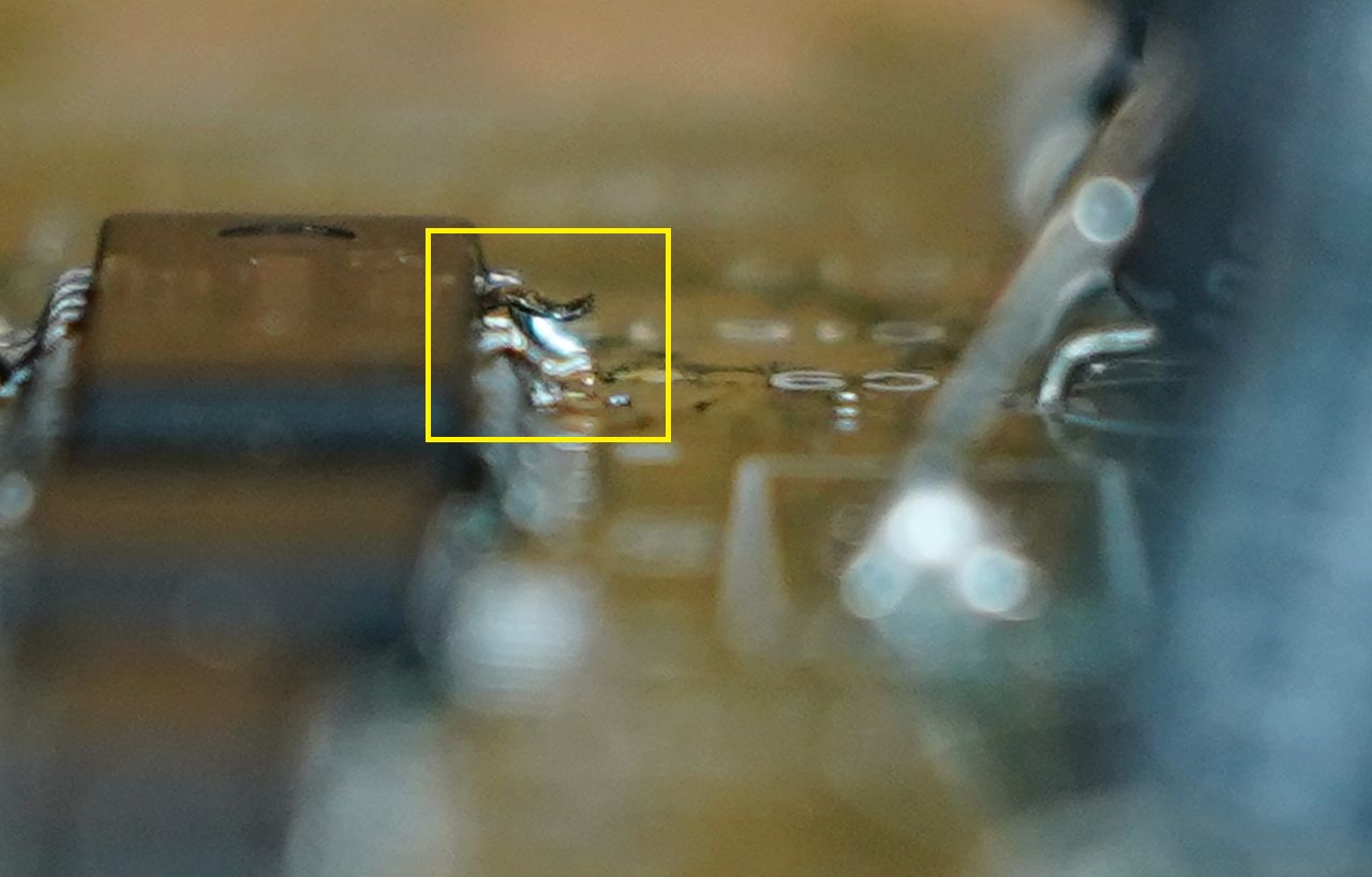
You must carefully lift pin 10 (SC) and pin 7 (LLCS). To do this you will want to add a small amount of solder to the pins, then while you have the pin heated with your soldering iron use something small like a needle or the tip of a pair of tweezers to pry underneath the pin and carefully lift it up by a couple of millimeters. Once you have lifted the pins you should use some desoldering braid to remove the excess solder from the pad underneath the pins you lifted. Once this is complete the pins should look similar to the following picture.
Step 12: Solder the Y and C wires to pins 17 and 12 respectively.
Step 13: Solder the LLCS wire and the SC wire to the lifted pins 7 and 10 respectively. Make sure to only solder the wires to the pins that you lifted and that the pads underneath them are not connected to anything.
Once you are finished soldering the S-Video wires, you should add some electrical tape to the 7805 heatsink as shown below to prevent any possible shorts.
Optionally you can also close the jumper labeled LPF_OFF, that will turn off the low pass filter built into the THS7374 amplifier chip. You may want to turn this off if you are outputting to a scaler that already has a low pass filter built in. Doubling up on the low pass filter could result in a softer image. If you are not outputting to a device with built in filtration then you will definitely want to leave this jumper open so the THS7374 can filter out all of the high frequency noise that would end up in your image if left unfiltered.
Step 14: Reassemble your SNES and enjoy!